 01
01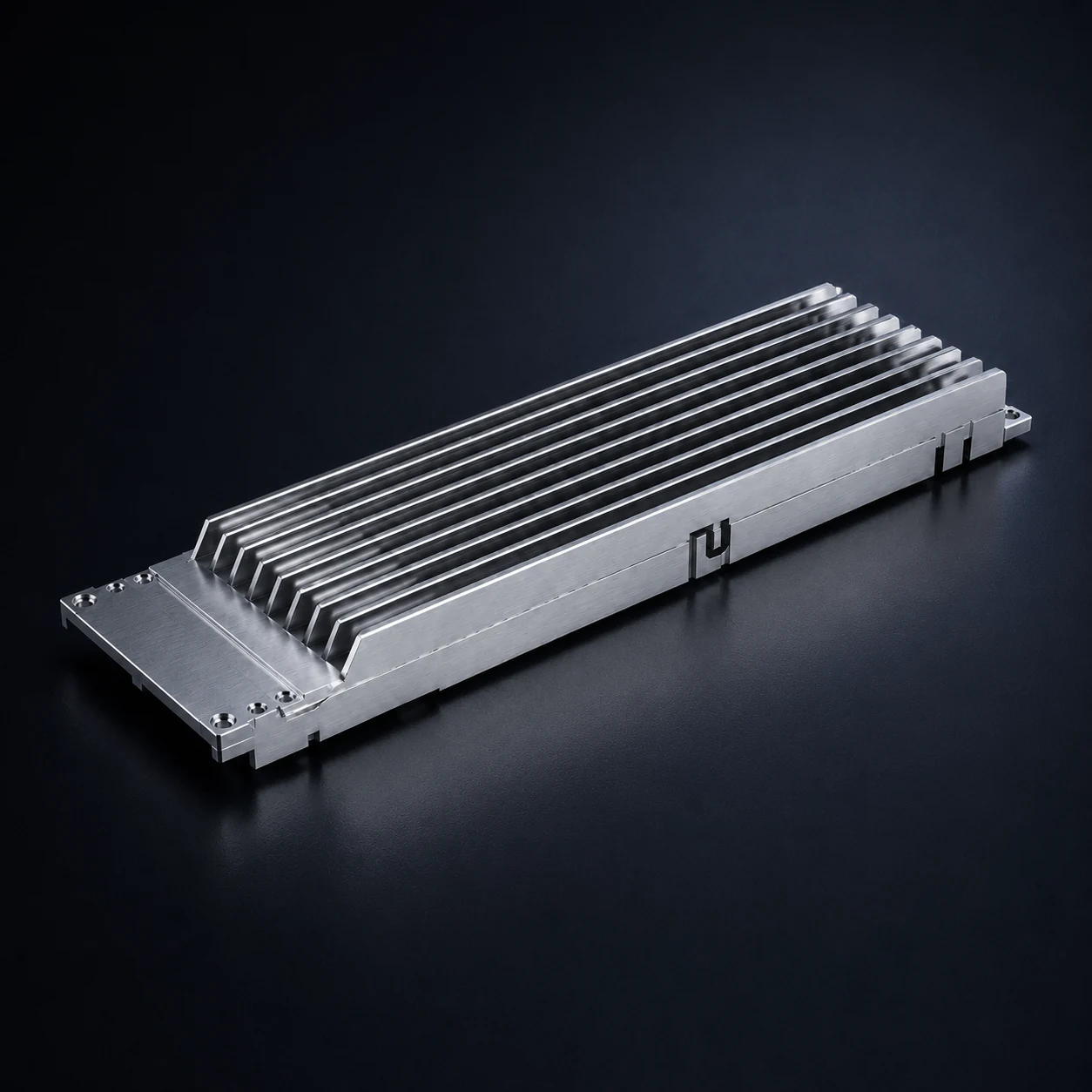
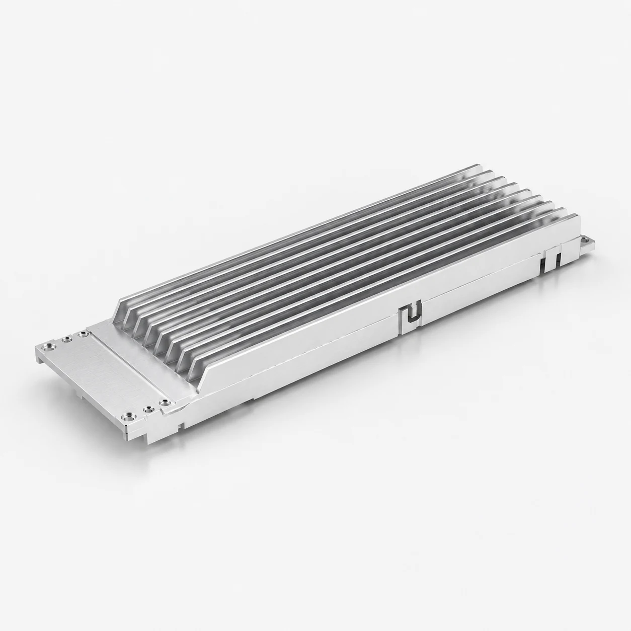
Extruded Heatsink Machining
Cutting, facing, holes, slots, mounting steps and locating features on aluminum extrusions.
Extrusion · CNC
Machining Fields / Optical Transceiver Thermal & Precision Parts
OPTICAL TRANSCEIVER THERMAL MANAGEMENT
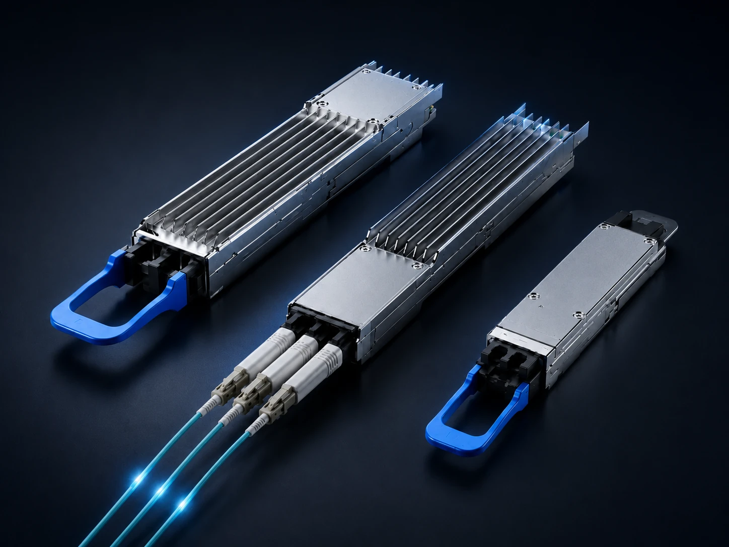
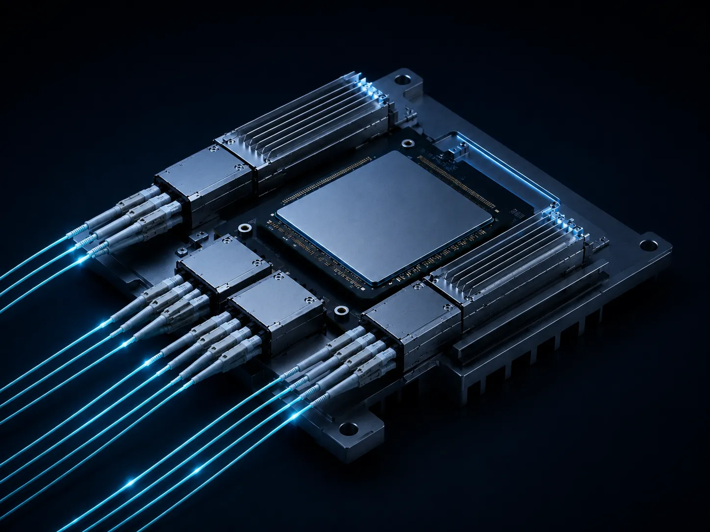
For 400G, 800G and 1.6T high-speed optical transceivers, we provide machining for thermal housings, heat spreaders, precision bases and related structural parts.
Heatsinks · Precision bases
Multi-face features · Single setup
Cutting · Facing · Holes & slots
Distortion control · Contact surfaces
Edge finishing · Clean delivery
Anodizing · Dimensional verification
OPTICAL TRANSCEIVER BASICS
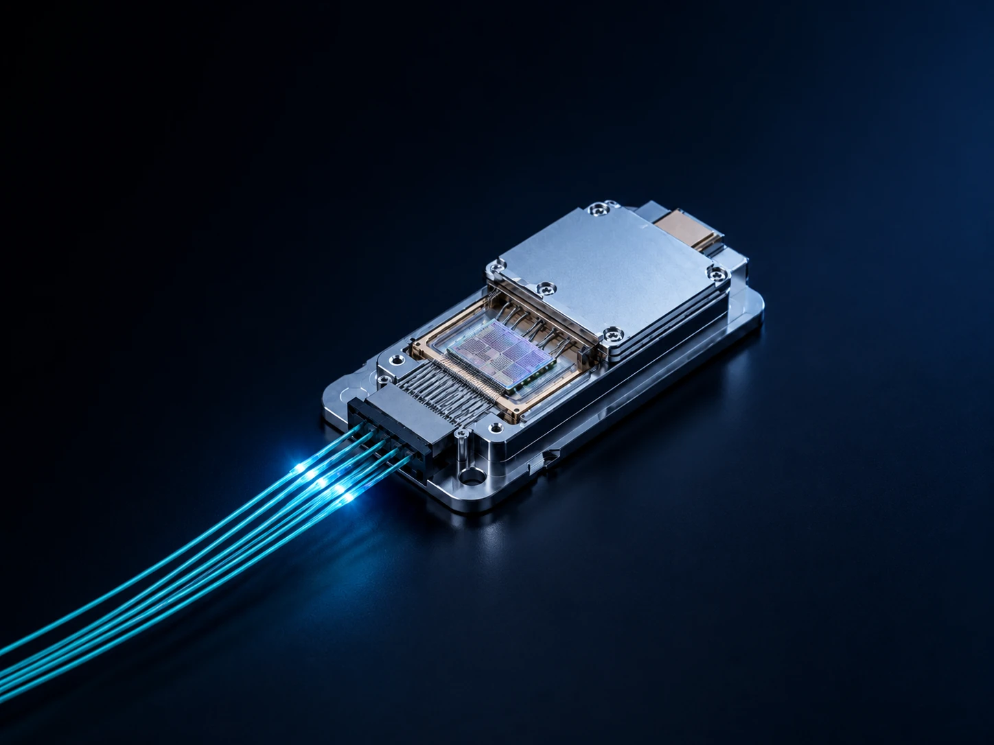
High-speed optical transceivers are optoelectronic conversion modules used in switches, AI servers and data center interconnects. A 400G, 800G or 1.6T transceiver integrates optical devices, driver ICs, DSPs, high-speed circuitry and connector interfaces within a highly compact package, resulting in increasing power density and thermal load.
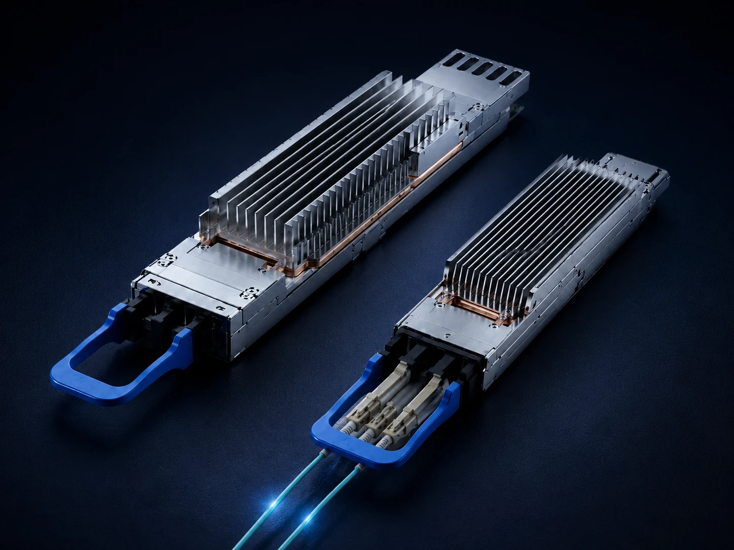
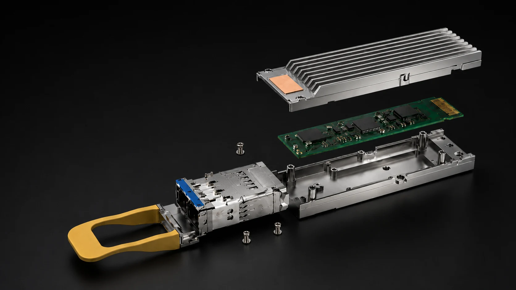
Heat generated by the main chips must pass through thermal interfaces and heat-spreading contact surfaces to the upper heatsink. The heatsink, precision base, locating housing and connector structure jointly determine thermal resistance, contact flatness, assembly datums and long-term reliability. These parts may be produced through secondary machining of aluminum extrusions, finish machining of formed blanks or complete CNC machining.
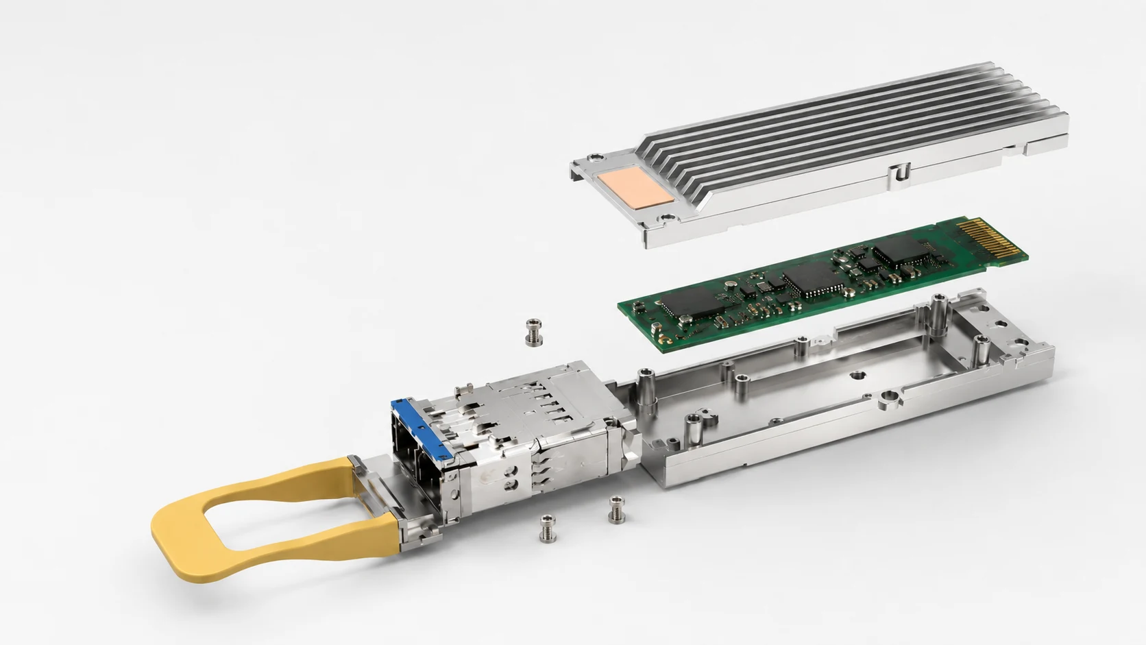
Upper Heatsink
Transfers chip heat
Chips & PCB
Primary heat sources
Precision Base
Mounting and datums
Latch & Interface
Insertion and retention
MACHINING SCOPE
Machining support for high-speed optical transceiver thermal paths, assembly datums and lightweight structures, including secondary extrusion machining, complex cavities, precision contact surfaces and copper or aluminum thermal parts.
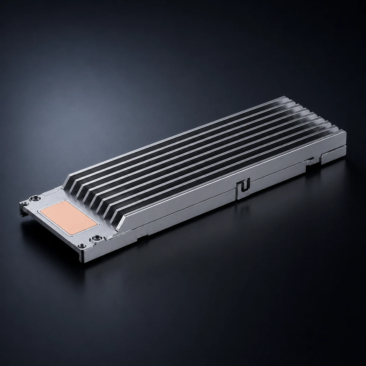
01Cutting, facing, holes, slots, mounting steps and locating features on aluminum extrusions.
 02
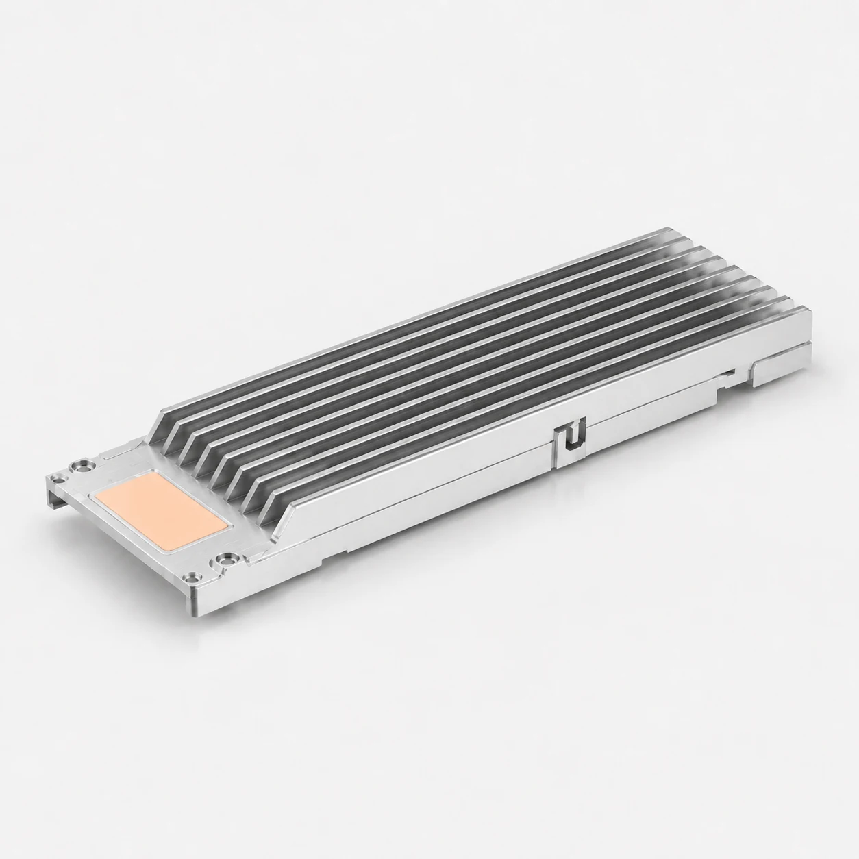
02Integrated fins, chip contact surfaces, mounting holes and locating structures.
 03
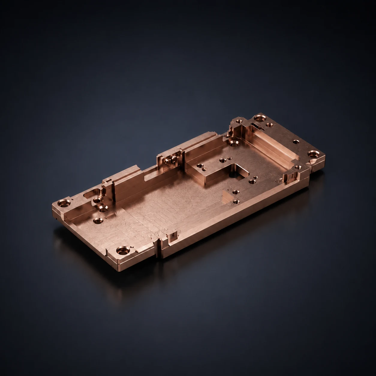
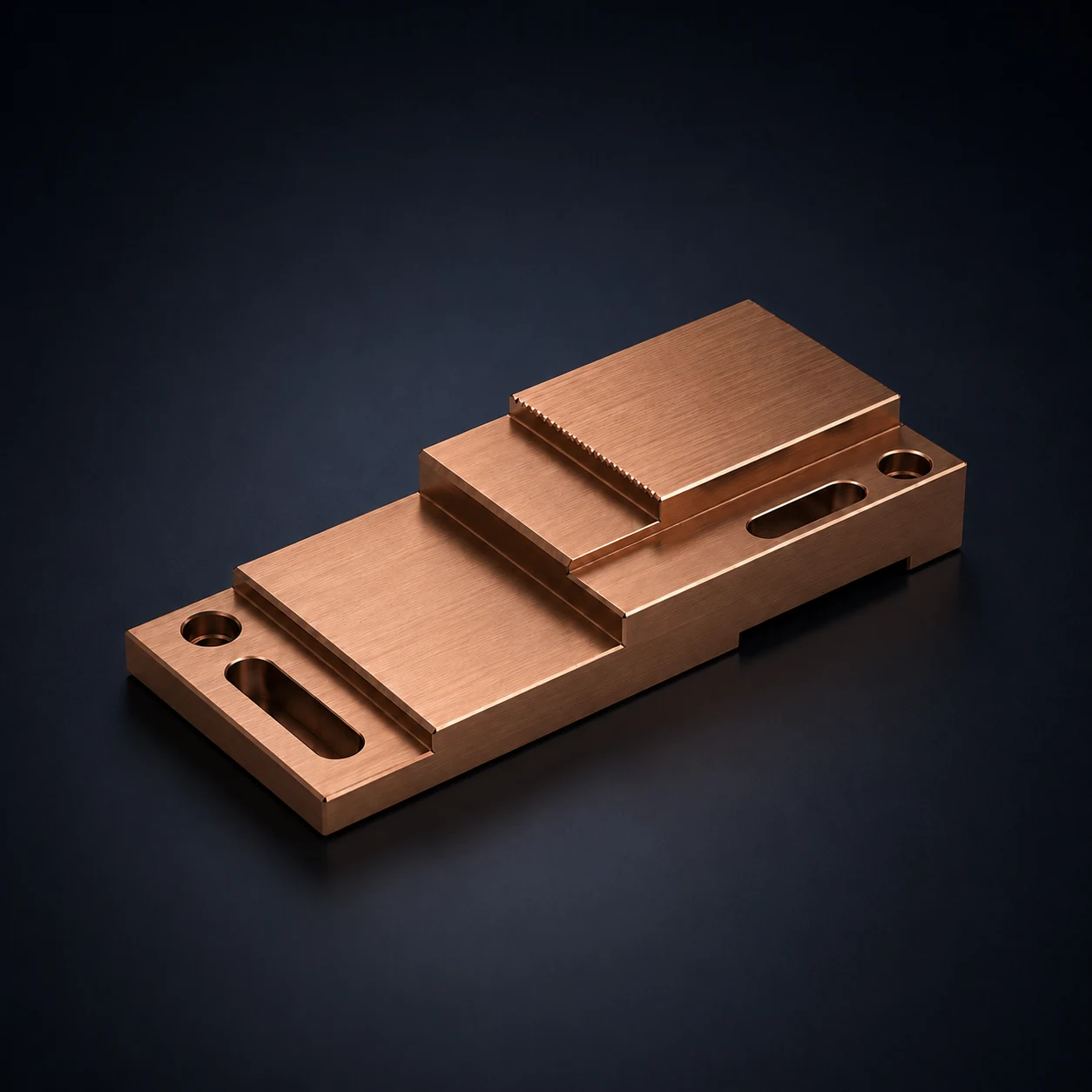
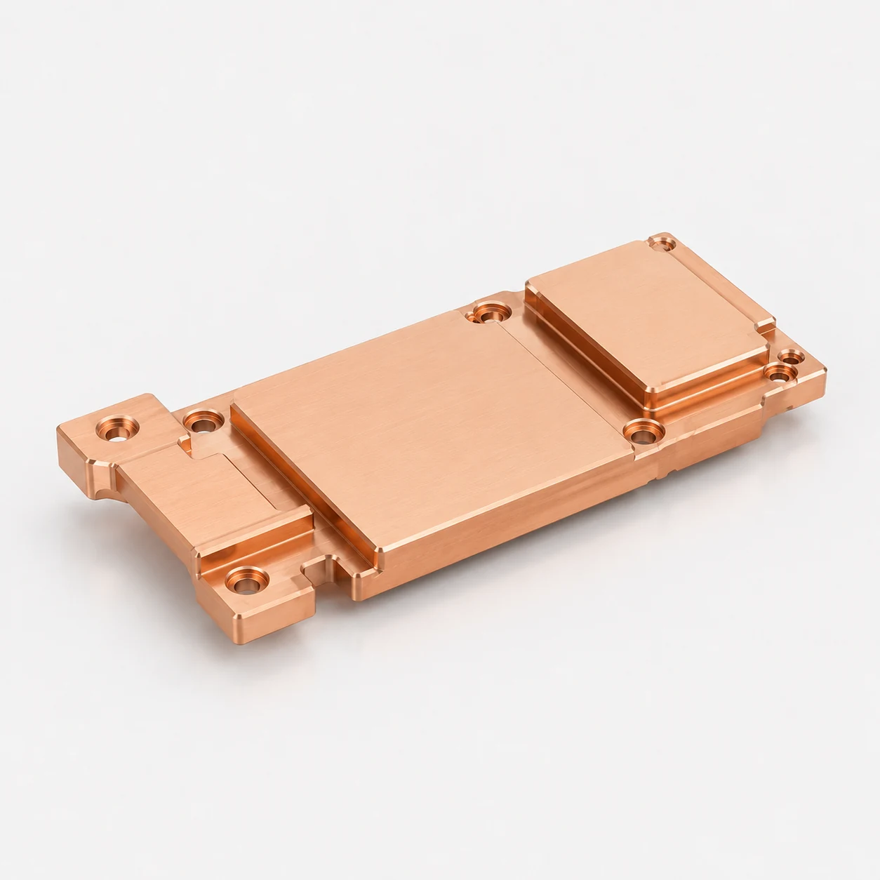
03Copper or aluminum contact plates with raised pads, stepped levels and controlled flatness.
 04
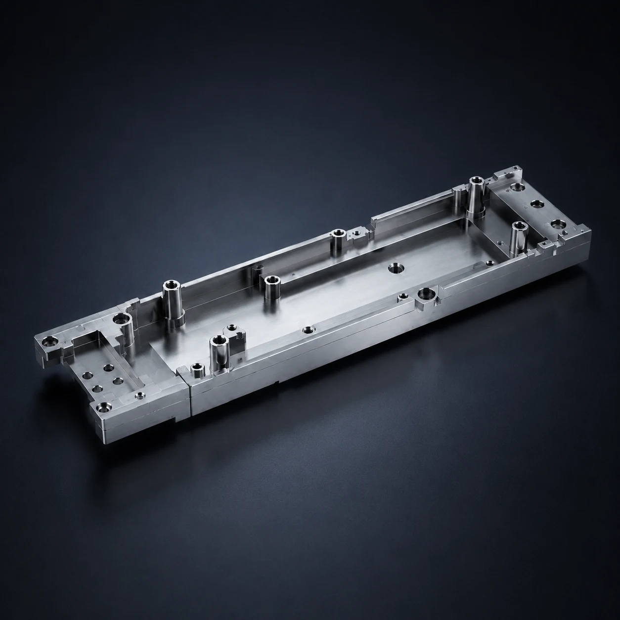
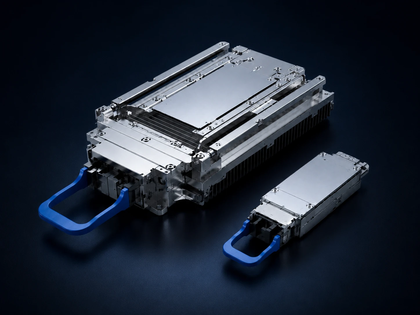
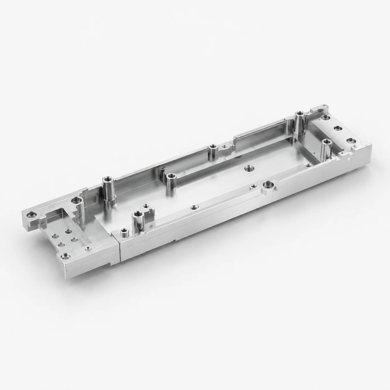
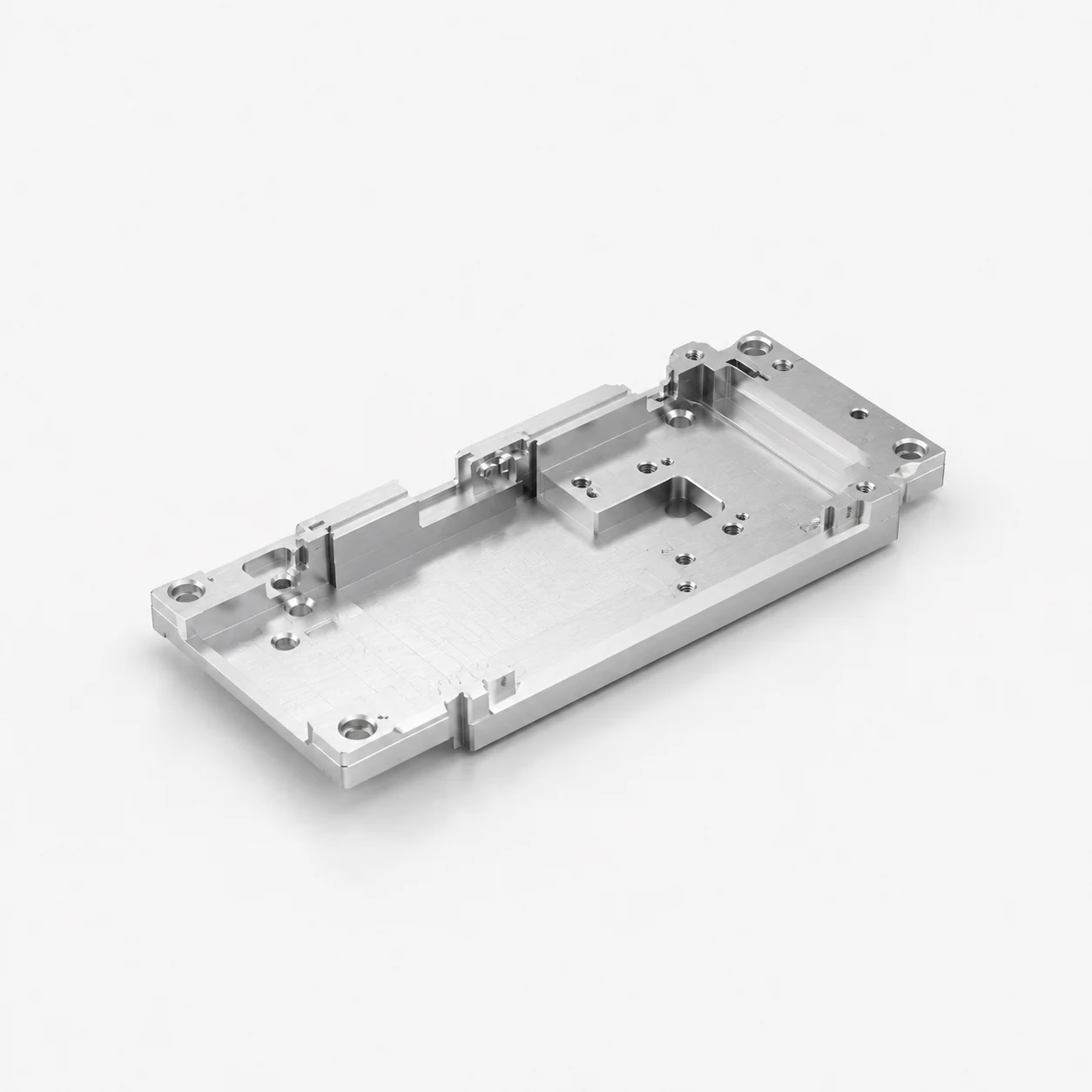
04Complex cavities, thin walls, locating bosses, threaded holes and PCB assembly datums.
 05
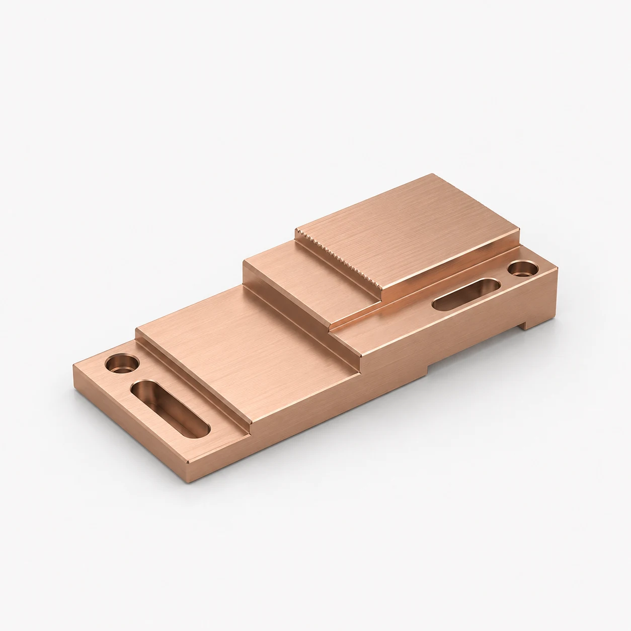
05Small precision slots, locating holes, mounting faces and optical assembly datums.
 06
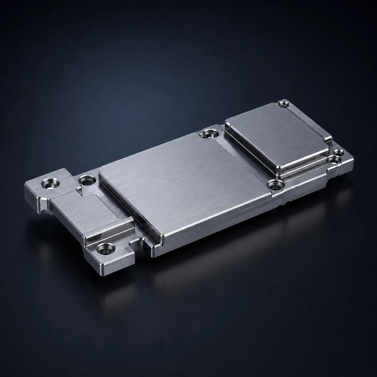
06Multi-height contact surfaces connecting heat sources, housings and upper heatsinks.
MANUFACTURING ROUTE
A complete process covering materials, precision machining, thermal contact surfaces, surface finishing and cleanliness control from engineering review to stable production.
Review materials, tolerances, thermal paths, contact faces, datums and machinability.
Select aluminum extrusion, aluminum plate, copper or composite thermal structures.
Complete stock cutting, rough milling, datum setup and machining allowance planning.
Validate process sequence, fixturing, tooling, distortion and dimensional stability.
Machine cavities, fins, thin walls, slots, datums and thermal contact surfaces.
Apply deburring, cleaning, electroless nickel, passivation or selective anodizing.
Inspect dimensions, flatness, roughness, cleanliness and production consistency.
APPLICABLE PRODUCTS
Precision thermal and structural parts for data-center interconnects, coherent communications and next-generation co-packaged optical architectures.
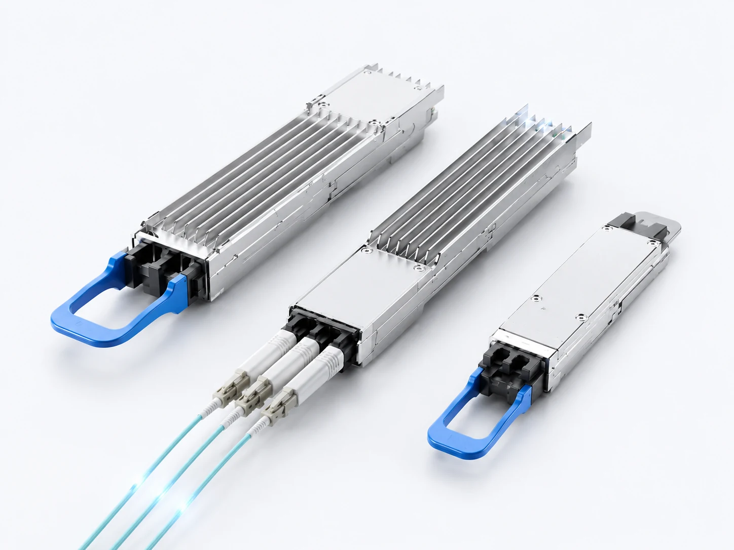 01
01Thermal lids, extruded heatsinks, precision bases and heat-spreader contact parts for QSFP-DD and OSFP modules.
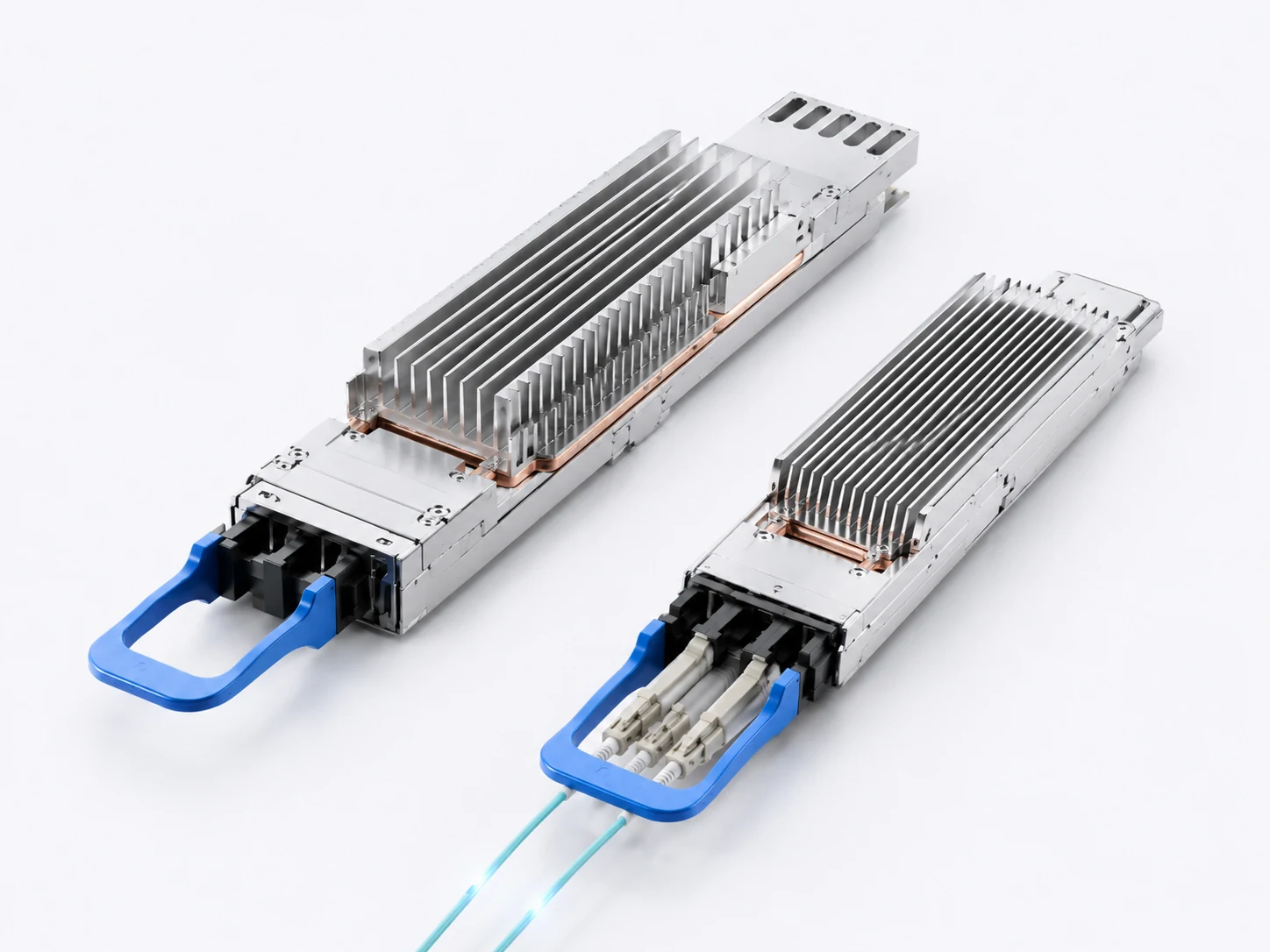 02
02Large-area heatsinks, stepped thermal blocks, copper heat spreaders and high-flatness contact surfaces.
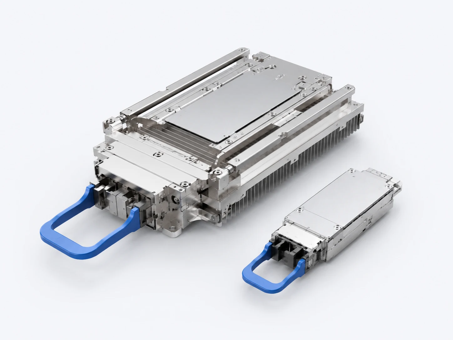 03
03Complex housings, optoelectronic mounting bases, heat-spreading structures and precision assembly datums.
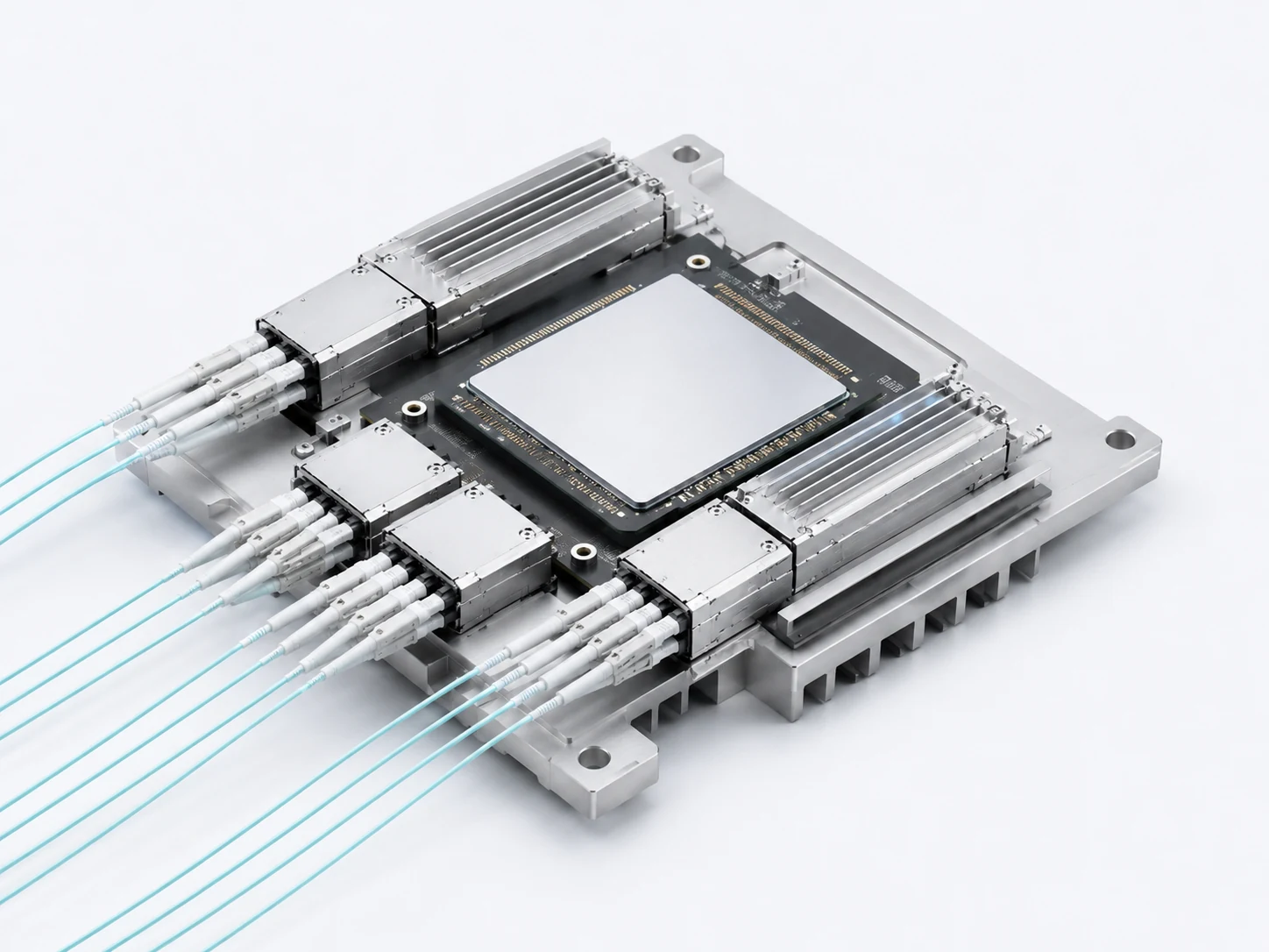 04
04Optical-engine mounts, thermal interfaces, cold-plate connection bases and precision locating parts.
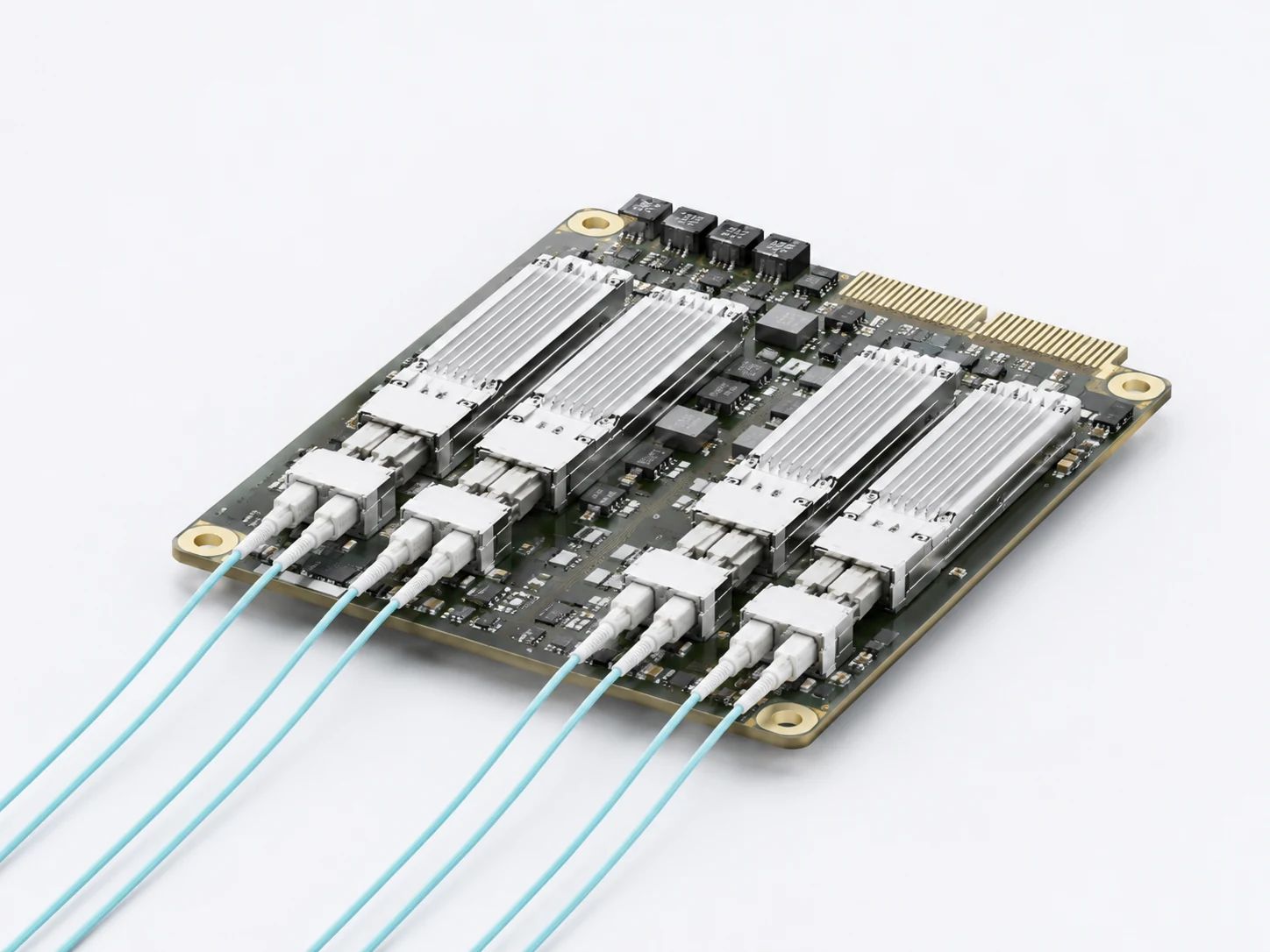 05
05Compact heatsinks, mounting bases, locating structures and PCB-level thermal management parts.
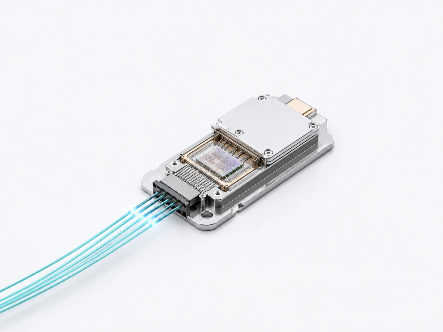 06
06Micro heat spreaders, silicon-photonics engine bases, fiber-array mounts and precision assembly parts.
CRITICAL TO QUALITY
| Critical Item | Why It Matters | Control Focus |
|---|---|---|
| Thermal Contact Flatness and Roughness | Directly affects real contact area, interface pressure and thermal contact resistance. | Control flatness, roughness, local high spots, tool marks, dents and the complete thermal interface area. |
| Datum and Positional Relationships | The housing, PCB, connector, optical engine and thermal surface must align in limited space. | Establish a common datum system and control holes, steps, end faces, total height and connector position. |
| Thin-Wall and Fin Distortion | Long housings, deep cavities and thin walls may warp after machining, unclamping or finishing. | Use balanced stock removal, separated rough and finish machining, stress relief and in-process flatness checks. |
| Surface Treatment and Thermal Interface Protection | Anodizing, electroless nickel and passivation change dimensions and surface contact conditions. | Separate cosmetic, corrosion-resistant, insulating and thermal surfaces, with masking and thickness compensation. |
| Burrs, Particles and Cleanliness | Debris, oil or micro-burrs can affect optical assembly, connector insertion, PCB reliability and TIM contact. | Control holes, slots, fin edges and cavities through deburring, cleaning, inspection and protected packaging. |
| Production Consistency and Traceability | Small dimensional drift can accumulate into assembly, insertion-force and thermal-performance variation. | Use first-article approval, in-process inspection, fixture verification, batch records and trend monitoring. |
ENGINEERING FAQ
Individual dimensions do not guarantee the complete mechanical envelope. Accumulated variation among connector position, PCB datum, housing height, thermal surface, latch geometry and coating thickness can cause interference or insufficient thermal contact.
The issue may come from poor flatness, uneven TIM thickness, insufficient clamping force, local high spots, heat-source offset or an interrupted thermal path. Thermal contact resistance must be evaluated together with heatsink capacity.
Not in every case. Anodizing improves corrosion resistance, insulation and appearance, but it changes dimensions and interface conditions. Thermal areas may require masking, controlled thickness, bare metal or another treatment.
Residual stress, unbalanced material removal, unclamping spring-back, treatment temperature, coating variation and inconsistent inspection support can all cause distortion. Inspection should be performed before and after finishing.
RFQ REQUIREMENTS
Complete drawings, thermal-interface data, assembly datums and finishing requirements support accurate process, risk, lead-time and production-cost evaluation.
PDF / DWG
STEP / IGES
Grade / Temper / Stock
Prototype / Pilot / Production
Tolerance / GD&T / CTQ
Flatness / Roughness / TIM
Anodizing / Ni / Masking
PCB / Cage / Connector
CMM / Flatness / Roughness
Cleanliness / Packing / Batch
TECHNICAL RESOURCES
Upload your drawings. Our engineering team will provide a manufacturing review and quotation within 24 hours.