In This Article
Direct conclusion
An optical transceiver thermal contact surface is a functional interface in a complete heat path:
Heat-generating IC / optical engine
→ internal heat spreader
→ module thermal lid or spreader plate
→ TIM
→ riding heatsink or system cold plate
→ air or liquid-cooling system
The correct engineering sequence is not “make Ra as small as possible.” It is:
- define the allowable temperature rise and interface resistance;
- define the real contact area, assembly datums and normal load;
- control macro-gaps with flatness and waviness;
- control microscopic contact and TIM wetting with roughness and lay;
- select the TIM and control its final bond-line thickness;
- verify the interface again after finishing and under production assembly conditions.
| Control item | Primary function | Typical result when uncontrolled |
|---|---|---|
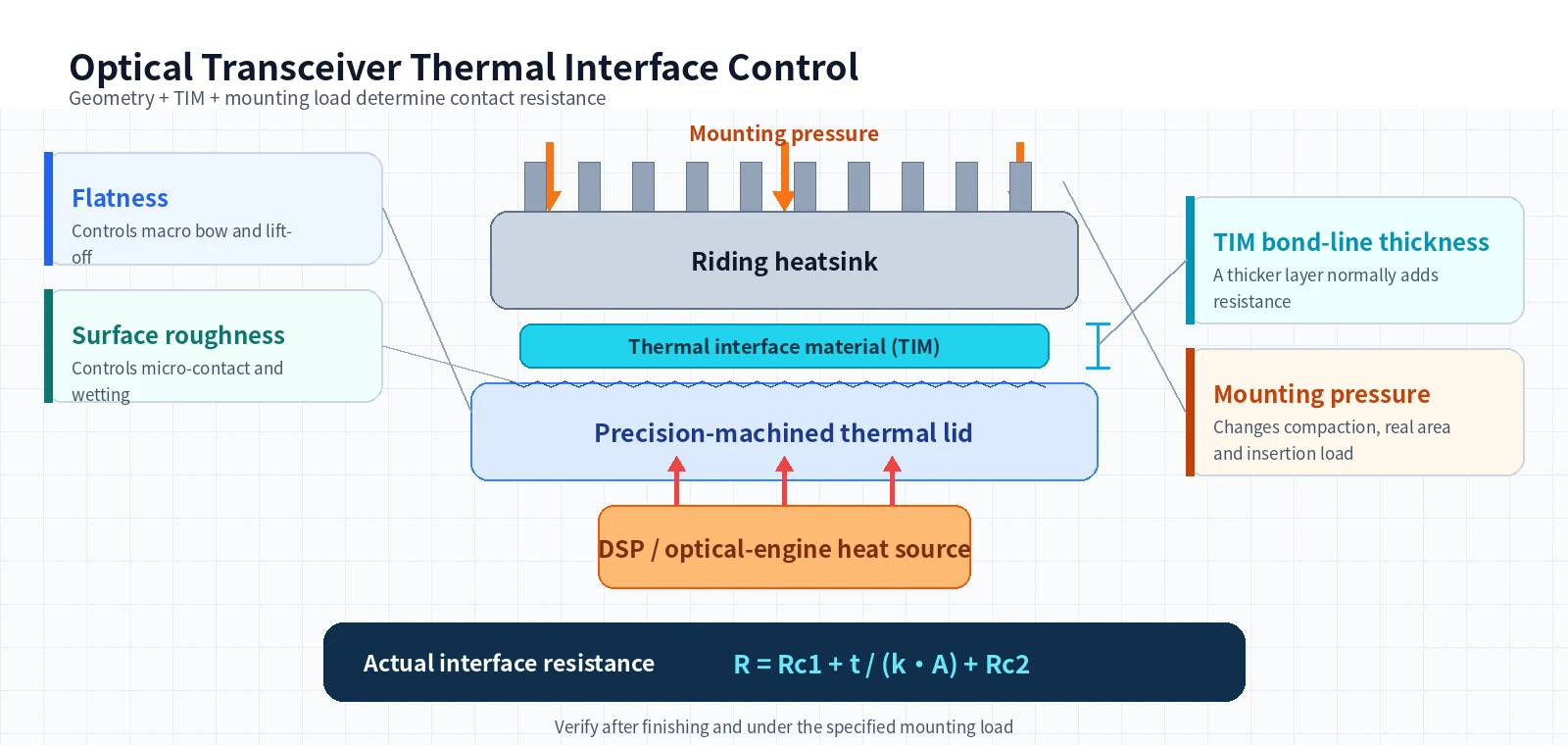
| Flatness | Limits bow, tilt and local lift-off | Nonuniform TIM and areas without contact |
| Roughness | Affects microscopic contact, wetting and trapped air | Variable contact resistance |
| TIM thickness | Fills residual gaps and forms the conductive layer | Excess thickness raises resistance; insufficient coverage creates voids |
| Mounting pressure | Compacts TIM and increases real contact area | Low pressure gives poor contact; excessive force damages the module or connector |
| Surface finish | Changes corrosion, insulation, dimensions and conduction | Coating enters the heat path or shifts functional height |
1. Why are high-speed optical modules increasingly dependent on the thermal interface?
A 400G, 800G or 1.6T module concentrates DSPs, drivers, lasers, receivers and high-speed circuitry within a small volume. As power and power density rise, heat must move rapidly to the top thermal surface and then into a riding heatsink, an integrated heatsink or another system-level cooling structure.
The conductivity of the aluminum or copper part itself is generally predictable. The larger uncertainty often lies at the contact between two solids. Surfaces that appear to touch are actually supported by a limited number of microscopic asperities, while the remaining area contains air. Because air is a poor conductor, even a small gap can create a significant temperature drop.
Pluggable optics add several constraints:
- the contact area is long and narrow and therefore sensitive to bow;
- riding heatsinks are spring loaded, while normal force is limited by insertion force, cage and connector loads;
- the interface must repeat after insertion and removal;
- labels, coatings, anodizing or local steps can enter the heat path;
- one lid may cover heat sources at different internal heights.
The interface must therefore satisfy thermal, mechanical, dimensional, insertion and lifetime requirements at the same time.
2. What makes up thermal contact resistance?
For a TIM between two metal surfaces, a simplified model is:
Rinterface = Rcontact-1 + tTIM / (kTIM × A) + Rcontact-2where:
Rcontact-1is the contact resistance at the first surface;Rcontact-2is the contact resistance at the second surface;tTIMis the final bond-line thickness, or BLT;kTIMis the bulk conductivity of the TIM;Ais the effective contact area.
This model highlights two common mistakes.
First, the conductivity printed in a TIM data sheet is not the final interface performance. A high-conductivity material can still perform poorly if the bond line is thick, compression is uneven or wetting is incomplete.
Second, machining quality affects the real area, BLT distribution and both contact-resistance terms. Part machining and TIM selection cannot be treated as independent tasks.
2.1 The real contact area—not the nominal area—governs the interface
A special issue of the Heat Transfer Society of Japan explains that two metal surfaces that appear to touch over a full area actually meet only at a limited number of microscopic asperities. The remaining nominal area contains air or TIM. Heat must constrict into those discrete spots and spread again on the other side, creating additional constriction and spreading resistance.
This leads to three practical conclusions for optical transceivers:
- Nominal area is not the same as real heat-transfer area. Flatness, waviness and isolated high spots change where and how many load-bearing contacts form.
- A small resistance can still matter at high power. Because
ΔT = Q × R, increasing module power can turn a seemingly minor interface resistance into a meaningful temperature rise. - Contact resistance is not a fixed material property. It changes with surface topography, normal load, TIM condition, temperature and assembly deformation, so a single constant in a simulation is not enough.
As bulk-material, heatsink and cold-plate resistances are reduced, the interface can represent a larger share of the total thermal path. Thermal-surface machining and assembly control should therefore enter the design and tolerance plan early rather than being treated as a final corrective action.
3. Flatness controls macro-gaps, not visual shine
Flatness describes whether the entire interface lies between two parallel planes. It governs overall bow, twist, edge lift and local high spots.
3.1 Common sources of flatness error
- extrusion bow and residual stress;
- stress release after rough machining a thin lid;
- heavy one-sided material removal;
- machining the part flat while it is clamped, followed by springback;
- distortion after anodizing, plating or heat exposure;
- deformation from screws or spring clips;
- differential thermal expansion in operation.
A drawing should therefore clarify:
- free-state or clamped-state inspection;
- machined condition or final finished condition;
- full interface or separate local thermal zones;
- parallelism or functional height relative to assembly datums;
- whether convexity, concavity or edge lift is restricted.
3.2 Use interface-specific standards as references, not universal defaults
The OIF thermal interface agreement for pluggable optics calls for reporting normal force, surface roughness and flatness. A specific CFP2-ACO interface recommendation has used flatness of 0.08 mm maximum and Ra of 0.8 μm maximum.
This confirms that both parameters matter, but the values belong to a particular interface size, force and module architecture. QSFP-DD, OSFP, custom heat spreaders and CPO optical engines may use different areas, loads and TIMs; one tolerance should not be copied across every design.
4. Roughness controls microscopic contact, but smoother is not automatically better
Roughness describes small peaks and valleys. Ra is common, but Ra alone does not reveal:
- isolated tall peaks;
- machining lay direction;
- periodic tool marks;
- waviness or local depressions;
- changes after surface finishing.
For thin grease, phase-change material or metal TIM, lower roughness often helps achieve a thin bond line and displace air. For flowable gels or interfaces that require resistance to sliding, some texture can aid wetting and retention. “Mirror finish” is therefore not a universal requirement.
The finish must match the TIM:
| Interface type | Main surface-control focus |
|---|---|
| Near-direct metal contact | Low asperity height, clean surfaces and adequate pressure |
| Thin grease / phase-change TIM | Low waviness and a stable thin bond line |
| Soft gap pad | Macro-gap and compression control; Ra is not the only driver |
| Dispensable thermal gel | Gap, dispense volume, spread, overflow and cured thickness |
| Metal foil or metal TIM | Surface compatibility, pressure, wetting and cycling reliability |
5. A TIM is not a universal shim for uncontrolled geometry
The TIM replaces air and accommodates a limited amount of micro- and macro-mismatch. Material families cover very different gap ranges.
5.1 Thin-interface materials
Greases and phase-change materials are commonly used where the mating surfaces are relatively flat and the bond line is thin. Industry guidance often places these materials around 50 μm or less, although the actual value must come from the specific material and assembly validation.
Advantages:
- low BLT and low bulk-layer resistance;
- good wetting of microscopic features;
- suitability for high heat flux.
Risks:
- sensitivity to flatness, dispense volume and pressure;
- local starvation if the layer becomes too thin;
- pump-out, dry-out or migration during thermal cycling.
5.2 Gap pads and gap fillers
Soft pads and gels can accommodate larger assembly gaps and component-height variation. They reduce the need for perfect coplanarity but create a thicker layer.
The design must define:
- nominal, minimum and maximum gap;
- target compression;
- reaction force on the PCB, optical devices and connector;
- compression set and thickness retention after cycling;
- height variation when one TIM covers multiple heat sources.
5.3 Metal TIMs
Indium foils, solder TIMs and liquid metals can deliver low resistance but require close review of surface metallization, corrosion, electrical risk, overflow, assembly process and rework. They are specialized solutions for demanding heat flux, not a default for every pluggable module.
6. Why must mounting pressure be defined together with flatness?
Additional normal pressure often:
- deforms asperities;
- promotes TIM wetting and spread;
- reduces effective BLT;
- increases real contact area;
- lowers contact resistance.
But a pluggable module cannot accept unlimited force. A riding-heatsink spring also loads the module housing, cage, PCB connector and insertion mechanism. Excessive force may cause:
- high insertion and extraction force;
- lid or base bending;
- stress on the PCB, connector or optical assembly;
- excessive TIM squeeze-out;
- unequal loading across multi-port cages.
The interface definition should combine:
Contact area
+ normal force or pressure range
+ TIM type and target BLT
+ flatness and roughness
+ allowable structural deformation
An Ra value without load and TIM conditions is not enough to predict resistance.
6.1 A compliant average load does not prove uniform contact pressure
The same HTSJ special issue describes a pressure-film method that maps local interface pressure rather than reporting only an average. The map identifies high-pressure, low-pressure and nearly unloaded regions and can then be related to local contact resistance.
This is highly relevant to a long, narrow transceiver lid. The total spring force may meet specification while lid concavity, isolated high spots or datum tilt concentrates the load at the ends or at a few points. Average force then looks correct even though real contact area and TIM compression are highly nonuniform.
During development, review these data together:
- free-state and assembled flatness;
- two-dimensional pressure-film or contact-print distribution;
- compressed TIM thickness and coverage;
- thermal-image, cold-plate or key-sensor temperature differences;
- spring force, clip location and load variation across multi-port cages.
This correlation separates a geometry problem from a spring-system, TIM-spreading or assembly-stack problem.
7. How should the thermal surface be defined on the drawing?
Treat the thermal interface as a CTQ rather than a general cosmetic surface.
| Drawing item | Information to define |
|---|---|
| Interface boundary | Functional heat-transfer area; whether labels or markings are permitted |
| Datum system | Relationship to module seating, connector and cage datums |
| Flatness | Free or assembled state; machined or final finished state |
| Roughness | Ra and, when needed, Rz, lay direction or prohibited defects |
| Height and parallelism | Thermal-surface height and tilt relative to assembly datums |
| Surface finish | Anodizing, nickel, conversion coating, masking or post-finish machining |
| Edge condition | Chamfers, burrs, dents, tool marks and masking boundaries |
| Cleanliness | Oil, chips, adhesive residue, oxidation and packaging protection |
| TIM condition | Type, area, nominal thickness, compression or dispense volume |
| Assembly load | Spring force, screw torque, pressure range or displacement control |
If one lid has multiple heat sources, define whether they are coplanar, stepped or use different TIM thicknesses. One overall flatness callout cannot replace local-height CTQs.
8. How can machining hold flatness and roughness in production?
8.1 Stock and residual stress
Thin lids, long spreader plates and aluminum extrusions are sensitive to residual stress. Production planning should consider:
- extrusion straightness and lot condition;
- roughing and finishing allowance;
- balanced material removal;
- aging or dwell after rough machining;
- flip sequence and clamping load;
- free-state verification before final machining.
8.2 Fixturing
A common false-flat condition occurs when a bowed part is pressed flat on the fixture, machined, and then springs back after release.
Avoid:
- excessive clamps close to the interface;
- forced flattening without free-state reinspection;
- unsupported thin walls;
- inconsistent clamp force in multi-part fixtures.
8.3 Finish machining
- use a stable cutter and controlled edge condition;
- standardize final allowance, direction and cutting parameters;
- control blend marks, chatter and isolated high spots;
- define tool-life and compensation rules;
- avoid hand sanding as a substitute for geometry control;
- monitor flatness, waviness and Ra together on long surfaces.
Hand polishing may reduce Ra while damaging flatness, edge height or local thickness. Visual brightness is not a valid acceptance method for a critical thermal surface.
9. Why must the interface be reverified after surface treatment?
Anodizing, electroless nickel, conversion coating and paint can change the interface by:
- adding thickness and shifting functional height;
- changing roughness and wetting;
- producing nonuniform build at holes, edges and steps;
- distorting a thin part during pretreatment or thermal exposure;
- leaving masking steps, residue or burrs.
Three common strategies are:
- Finish the thermal surface with the rest of the part—useful when insulation or corrosion protection is required, but include the coating in thermal and dimensional validation;
- Mask the thermal area—retains a metallic interface but requires control of the mask boundary, corrosion and cleanliness;
- Finish-machine after treatment—provides direct geometry and conduction, but requires protection of exposed metal, deburring and final cleaning.
Inspection must represent the delivered condition. A bare machined part does not represent the final treated interface.
10. How should flatness, roughness and real contact be inspected?
10.1 Flatness
Depending on area, tolerance and production rate, methods may include:
- CMM point-cloud inspection;
- height gauge on a granite surface;
- scanning profile or optical metrology;
- a dedicated functional gauge;
- displacement or contact-print inspection in the assembled state.
A small number of points can miss isolated high spots. Long or multi-zone surfaces need a defined point pattern or scan path and a consistent support condition.
10.2 Roughness
A profilometer setup should standardize:
- measurement location;
- sampling length and cutoff;
- direction relative to machining lay;
- filtering settings;
- pre- or post-finish condition.
10.3 BLT and contact
- control BLT through the tolerance chain or spacer beads;
- record dispense mass, path and area;
- use pressure film or contact prints to check load distribution;
- section development samples to examine voids and thickness;
- inspect pump-out, migration and compression set after cycling;
- measure temperature under real module power and airflow or cold-plate conditions.
11. Material testing and module-level thermal validation are not interchangeable
ASTM D5470 characterizes steady-state thermal transmission through TIM specimens and can produce thermal impedance or apparent conductivity data. It is useful for comparing materials and creating model inputs, but its test surfaces, pressure, thickness and temperature may differ from the module.
Assembly-level validation should also cover:
- actual interface area;
- heatsink normal force;
- lid flatness and roughness;
- real BLT;
- module power and hotspot distribution;
- repeatability after insertion and removal;
- drift after high/low temperature and thermal cycling;
- interaction across multi-port cages.
The OIF optical-module thermal interface method uses a cold plate and requires the relevant geometry and load data to be reported. That approach is closer to the real engineering problem than comparing conductivity values alone.
11.1 High-heat-flux testing must also monitor the TIM’s material state
High-heat-flux experiments summarized in the HTSJ issue show that a TIM can reduce contact resistance and suppress its deterioration as heat flux rises, but performance is not determined by nominal conductivity alone. Whether the material remains continuous, wets the surfaces, hardens or changes phase, and whether voids develop can change the measured resistance.
Optical-transceiver TIM validation should therefore cover:
- real operating power and short-duration heat-flux peaks;
- cold start, steady high temperature and post-cycle interface condition;
- BLT and rebound before and after compression;
- pump-out, migration, cracking, hardening and void formation;
- repeatability after module insertion or heatsink removal and reassembly.
Solder, metal-paste and phase-change interfaces also require checks for phase behavior, surface compatibility and rework-induced voids. High conductivity is a material capability; a stable interface is a system capability.
12. Six common failure modes
| Failure mode | Root cause | Direction for improvement |
|---|---|---|
| Contact at both ends but lift-off in the middle | Long-axis concavity or forced flattening in the fixture | Control free-state flatness and residual stress |
| Thin TIM on one side and thick TIM on the other | Thermal surface tilted relative to assembly datums | Add height, parallelism and stack-up control |
| Ra passes but thermal resistance varies | High spots, waviness or contamination | Add surface-form and cleanliness control |
| A higher-conductivity TIM raises temperature | BLT, pressure or spread no longer matches | Compare resistance under the real assembly condition |
| Failure after anodizing or plating | Coating thickness, masking step or distortion omitted | Inspect in the final finished condition |
| Prototype passes but production drifts | Tooling, clamping, dispense or spring-force variation | Establish CTQs, SPC and reaction plans |
13. What information is needed for RFQ and DFM review?
Provide:
Module type and power
Heat-source position and interface area
2D drawing and 3D model
Material and stock condition
Thermal-surface datums, flatness and roughness
Surface finish and masking
TIM type, thickness or compression
Heatsink normal force or assembly method
Prototype, pilot and production quantities
Inspection report and thermal-validation requirements
If the surface requirement is not frozen, provide the target temperature rise, contact area, available load and assembly gap so thermal, mechanical, TIM and manufacturing teams can develop a manufacturable specification together.
14. Final engineering recommendations
The objective is not a metal surface that merely looks flat and bright. It is a low-resistance interface that remains stable under the specified load, TIM, finish and production variation.
Use these principles:
- Define target resistance and assembly conditions before allocating flatness and roughness.
- Treat BLT as a tolerance-chain result, not a TIM-supplier-only parameter.
- Manage the thermal surface as a CTQ and reinspect after finishing.
- Validate flatness, waviness, Ra, cleanliness and mounting load as one system.
- Use material data as an input; confirm the final result with assembly-level thermal testing.
- Control tool life, clamp force, dispense quantity, spring force and changes in production.
A robust interface must be thermally efficient, mechanically compatible, insertable, inspectable and repeatable in production—not rescued by extreme tolerances or an unnecessarily thick TIM.
Frequently Asked Questions
What flatness and roughness should an optical transceiver thermal surface specify?
There is no universal value. The requirement must be based on module geometry, interface area, TIM type, allowable load and target resistance. Some specific OIF module specifications have used flatness of 0.08 mm maximum and Ra of 0.8 μm maximum, but this is an interface-specific example rather than a default for every QSFP-DD, OSFP or custom module.
Is a smoother thermal contact surface always better?
No. Lower roughness often helps thin TIMs or near-direct contact, but performance also depends on waviness, machining lay, TIM wetting and mounting pressure. Reducing Ra without controlling overall flatness and isolated high spots can still produce nonuniform contact.
Can a thicker TIM compensate for poor flatness?
A TIM can accommodate a limited gap, but added thickness normally increases bulk-layer resistance and can introduce uneven compression, pump-out, mechanical stress or long-term thickness drift. Geometry should be controlled first, followed by a TIM selected for the remaining gap and reliability requirements.
Should an anodized layer remain on an aluminum thermal contact surface?
Not automatically. Anodizing provides corrosion resistance and electrical insulation but also changes interface conduction, roughness and dimensions. Critical thermal areas may be masked, locally stripped or finish-machined after treatment, subject to corrosion, electrical, cleanliness and assembly requirements.
How should TIM and thermal contact resistance be verified?
Separate material-level testing from assembly-level validation. ASTM D5470 can characterize steady-state TIM impedance and apparent conductivity, but the actual module should also be tested with its real area, mounting load, bond-line thickness, surface condition and heat flux using a cold-plate or application-level thermal method.