In This Article
Direct answer
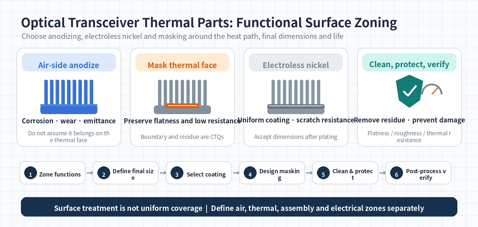
Surface finishing on an optical transceiver thermal component is a functional zoning problem, not a cosmetic operation applied uniformly to the whole part.
Air-side fins and external surfaces
→ corrosion, wear, appearance and radiation

Thermal contact surfaces
→ flatness, roughness, contact resistance and scratch resistance

Precision fits and assembly datums
→ final dimensions after coating

Grounding and EMI contact areas
→ electrical continuity and low contact resistance
A mature design may therefore combine anodizing, electroless nickel, masked bare metal and post-treatment machining on the same component.
| Functional zone | Common approach | Main risk |
|---|---|---|
| Air-side fins and exterior | Clear or black anodizing | thermal-cycle cracking, color and distortion |
| TIM or dry-contact surface | masked bare aluminum, selective coating or post-finish machining | contact resistance, scratches and contamination |
| Complex cavities and corrosion-critical areas | electroless nickel | pretreatment, phosphorus, thickness and final size |
| Threads, locating holes and grounding pads | masking or selective finishing | bleed, dimensional change and poor conductivity |
1. Why surface treatment is part of thermal management
The OIF thermal interface specification for pluggable optics treats surface material, flatness, roughness, spreading resistance and normal force as cumulative contributors to interface thermal resistance. Surface finishing is therefore not an independent cosmetic step after machining; it changes the thermal path.
It can affect:
- real contact between the thermal face and TIM;
- coating thickness and assembled height;
- bores, slots, threads and locating dimensions;
- hardness, wear and scratch resistance;
- electrical insulation or continuity;
- corrosion, cleanliness and long-term stability;
- coating integrity and part flatness after thermal cycling.
A drawing should answer three questions:
- Which areas must be treated and which must remain untreated?
- Are critical dimensions accepted before or after treatment?
- Does the thermal path rely on bare metal, a coating, or a TIM?
2. Anodizing: useful on air-side surfaces, but not automatically on every thermal face
Anodizing converts the aluminum surface into an aluminum-oxide layer. It is widely used to improve corrosion resistance, wear resistance, electrical insulation and appearance. It also raises thermal emittance, which is why anodized aluminum is common on heatsinks and enclosures.
2.1 What anodizing contributes
For optical transceiver thermal parts, anodizing can:
- protect extruded or machined aluminum from oxidation and corrosion;
- improve wear resistance on fins, rails and exterior surfaces;
- create an electrically insulating surface;
- provide stable color and visual identification;
- improve radiative heat rejection where radiation is meaningful.
Most data-center transceiver cooling, however, is dominated by conduction and forced convection. A black finish cannot compensate for poor airflow, weak fin design or a high-resistance thermal interface.
2.2 Why an anodic film can increase interface resistance
Aluminum conducts heat well, while the anodic oxide is much less conductive and electrically insulating. The film is thin, but it can still matter at a high heat flux, small interface area and limited contact force.
Extra caution is appropriate when:
- the module and riding heatsink use dry contact;
- the TIM bond line is very thin;
- normal force is limited by insertion or cage mechanics;
- the surface also provides grounding or EMI continuity;
- flatness, roughness and overall height are tightly controlled.
The correct decision balances corrosion and scratch protection against added thermal resistance, dimensional change and electrical isolation.
2.3 Thermal cycling and cracking
Sanwa Plating explains that the aluminum substrate and anodic film have different coefficients of thermal expansion. At elevated temperature, the brittle oxide may crack because it cannot follow substrate expansion. The company gives about 100 °C as a practical reference at which cracking may begin for a general anodic coating. This is not a universal design limit: alloy, film thickness, sealing, process route, peak temperature and cycle count must be evaluated for the actual application.
Dyed anodic finishes can also fade when organic dyes are exposed to heat. Color is not normally a thermal CTQ, but a change can indicate process or environmental variation.
3. Clear, black and hard anodizing
| Finish | Typical purpose | Engineering note |
|---|---|---|
| Clear anodize | corrosion resistance, insulation and general appearance | suitable for many fins and outer surfaces |
| Black anodize | appearance and higher surface emittance | do not use color alone as a thermal-performance claim |
| Hard anodize | higher hardness and wear resistance | greater dimensional and stress effects on precision features |
The alloy matters. 6063 extrusion and 6061 machined stock can differ in color and film appearance. Silicon, copper and porosity in cast aluminum also affect anodizing. Copper-aluminum assemblies need protection from trapped process chemistry and galvanic exposure at joints.
4. Electroless nickel: uniform coverage of complex shapes, but still a dimensional and thermal layer
Electroless nickel deposits a Ni-P alloy by chemical reduction without external current. Its major benefit is relatively uniform thickness on complex shapes, so it is common on precision components, cavities and surfaces requiring corrosion or wear resistance.
ISO 4527 and ASTM B733 treat autocatalytic nickel-phosphorus as an engineered coating with defined requirements and tests. For aluminum, ASTM B253 emphasizes pretreatment, cleaning, activation and zincate or strike procedures needed for adhesion.
4.1 Suitable applications
- complex cavities, steps and hole edges requiring uniform coverage;
- lids or heat spreaders requiring corrosion and scratch protection;
- copper or aluminum parts requiring a more stable surface state;
- features where final dimensional consistency matters;
- dry-contact areas exposed to insertion, wiping or cleaning.
4.2 Uniform thickness does not remove dimensional control
The coating adds thickness to every unmasked surface:
- outside diameters grow;
- bores become smaller;
- slots and step heights change;
- overall contact height, flatness and roughness can change;
- mask boundaries can create transition zones or local build-up.
Functional dimensions should normally be defined and accepted in the post-plating condition.
4.3 Phosphorus content and heat treatment
Phosphorus content changes hardness, corrosion resistance, magnetic behavior and chemical resistance. The drawing should therefore specify more than “electroless nickel”:
- phosphorus class or range;
- thickness and tolerance;
- whether heat treatment is required;
- adhesion, hardness and corrosion requirements;
- magnetic or electrical restrictions;
- final roughness and flatness of the thermal face.
Electroless nickel baths also operate at elevated temperature. Thin lids, long heatsinks and heavily machined parts can release residual stress during the process, so post-treatment inspection is essential.
5. Is electroless nickel always better than anodizing on a thermal face?
No. Electroless nickel is often more conductive and wear resistant than an anodic film, but it is still an added material layer. Final performance depends on:
substrate flatness
+ coating thickness and uniformity
+ post-plating roughness
+ hardness and scratch condition
+ TIM thickness
+ assembly pressure
A patent addressing dry-contact optical-module thermal faces proposes a transition layer and hard protective layer, with the final protective surface controlled to Ra 0.4 μm or less. It is not a general industry requirement, but it illustrates the key conflict in a pluggable module: the surface must be smooth enough for low contact resistance, hard enough to resist repeated insertion scratches and corrosion resistant enough to preserve its condition over life.
6. Masking is part of process design
Sanwa defines masking as covering areas that should not receive plating or anodizing. Typical methods include resist paint, tape, elastomer plugs and dedicated fixtures.
Common masked zones on optical transceiver parts include:
- module-to-heatsink thermal faces;
- grounding, shielding and spring-contact pads;
- locating holes and precision fits;
- threads and fastener seats;
- seal grooves, bonding areas and laser-weld zones;
- soldering, brazing or conductive-adhesive areas.
6.1 Define the boundary on the drawing
A note that only says “do not coat thermal face” is insufficient. Define:
| Item | Recommended definition |
|---|---|
| Datum | hole, face or centerline locating the mask |
| Boundary | size and allowable shift of treated/untreated zones |
| Radii and holes | whether coating may enter chamfers, radii or openings |
| Edge quality | limits for bleed, burr, staining, rack marks or flow marks |
| Final dimensions | acceptance before or after treatment |
| Cleanliness | no adhesive, oil, wax, silicone or cleaner residue |
Complex, deep or very small boundaries increase masking labor and defect risk. Repeatable plugs, caps and fixtures are usually better for volume production than hand-applied tape alone.
7. Protecting the thermal face from machining through customer assembly
An untreated thermal face still needs controlled protection. Risks include:
- scratches and dents during handling;
- process-solution leakage under the mask;
- adhesive residue;
- fingerprints, oil, abrasive particles and polishing compound;
- plasticizer or silicone transfer from packaging;
- oxidation after cleaning;
- probe marks and fixture damage during inspection.
A controlled route is:
final machining
→ cleaning and DI-water rinse
→ 100% visual check
→ temporary mask or protective film
→ surface treatment
→ mask removal
→ secondary cleaning
→ flatness / roughness / dimensional recheck
→ low-residue, silicone-free protective packaging
Protective films and tapes must be qualified for residue, compatibility with TIM and effect on the final surface.
8. Functional selection matrix
| Area | Preferred starting point | Comment |
|---|---|---|
| Fins and exterior | anodizing | corrosion, wear and emittance benefit |
| TIM contact area | masked bare aluminum, controlled anodize or electroless nickel | validate actual thermal resistance and life |
| Sliding dry-contact face | electroless nickel or another wear-resistant finish | control scratches, friction and roughness |
| Grounding/EMI pad | bare metal or conductive finish | anodic oxide is insulating |
| Precision bore/thread | masking or dimensional compensation | accept in final treated condition |
| Bonding/welding zone | usually masked | coating may reduce bond or weld quality |
9. Recommended process route
Prototype stage
- machine the geometry and thermal face;
- keep comparison samples with different finishes;
- test bare aluminum, selective anodizing and electroless nickel;
- compare temperature using the real TIM, force, power and airflow;
- test insertion wear, thermal cycling, humidity and cleaning compatibility.
Production stage
material and blank verification
→ rough machining and stress stabilization
→ finish machining of datums and thermal faces
→ pre-treatment dimensional inspection
→ cleaning, racking and masking
→ anodizing or electroless nickel
→ mask removal and cleaning
→ post-treatment dimensions, flatness, roughness and thickness
→ thermal sampling and protected packaging
OIF recommends revalidation when module material, surface specification or production method changes significantly. A new anodizing supplier, different Ni-P chemistry, altered thickness or new masking method should therefore be treated as an engineering change, not only a cosmetic change.
10. Post-treatment CTQs
| CTQ | Typical method | Production focus |
|---|---|---|
| Thermal-face flatness | CMM, flatness measurement or optical scan | define free and assembled condition |
| Surface roughness | profilometer with direction and location | measure after coating and mask removal |
| Coating thickness | XRF, eddy current or section | multiple positions and boundary areas |
| Mask boundary | visual and vision measurement | shift, bleed and edge defects |
| Functional dimensions | gauges, thread gauges and CMM | accept after surface treatment |
| Cleanliness | wipe, ionic or particle inspection | no adhesive, oil, silicone or polish residue |
| Adhesion/corrosion | specification-based adhesion and environmental tests | link to alloy, pretreatment and thickness |
| Actual thermal resistance | cold-plate or system test | use production TIM, force and power |
11. Common failures
| Failure | Common cause | Improvement |
|---|---|---|
| flatness fails after anodize | etching, thin-wall movement or racking stress | separate rough/finish stages and remeasure after treatment |
| thermal resistance increases | coating on face, residue, scratches or roughness | redefine masking and final cleaning |
| electroless nickel blisters | poor aluminum activation or contamination | control zincate/strike and adhesion tests |
| threads or bores bind | no thickness compensation or mask leakage | design for post-coating size and use gauges |
| mask edge stains or corrodes | chemistry trapped under mask or residue | improve boundary, plugs and cleaning |
| black-anodize color varies | alloy, surface, thickness or dye variation | standardize material and pretreatment |
| cracks after thermal cycling | substrate/film CTE mismatch | validate temperature, thickness, sealing and cycles |
12. RFQ and drawing inputs
Provide at least:
- substrate alloy, temper and blank route;
- anodize type, color, thickness and sealing;
- Ni-P class, thickness and heat treatment;
- mandatory treated and untreated zones;
- masking boundaries and datums;
- thermal-face flatness, roughness and cleanliness;
- final requirements for holes, threads, grounding and weld areas;
- dimensional acceptance state;
- thermal cycling, humidity, salt spray, insertion and thermal tests;
- prototype, pilot and production quantities.
13. Zhongde Precision engineering approach
For heatsinks, heat-spreading lids and precision optical transceiver housings, our DFM review links:
- machining datums to post-treatment acceptance datums;
- air-side, thermal, electrical and assembly zones;
- anodizing, electroless nickel and masking strategy;
- coating thickness to tolerance stack and contact height;
- thin-wall distortion before and after treatment;
- thermal-face cleaning, protection, packaging and final validation.
A stable production route is not defined only by what the finishing supplier can apply. Design, CNC machining, finishing, inspection and assembly must work to the same CTQs.
Frequently asked questions
Should an optical transceiver heatsink be anodized over the entire part?
Not automatically. Air-side fins and external surfaces are often suitable for anodizing, while TIM contact areas, dry-contact thermal faces, grounding pads, precision fits and threads need separate review. A critical thermal face may be masked, coated to a controlled thickness, given another finish, or finish-machined after treatment. The decision should be verified using final dimensions and actual assembled thermal resistance.
Does black anodizing always cool better than clear anodizing?
Black or other anodic finishes can increase surface emittance, but conduction and forced convection usually dominate optical transceiver cooling. Color alone does not determine performance. Fin geometry, airflow, interface resistance, coating condition and ambient temperature are more important, and a low-conductivity film on the contact surface may offset any radiation benefit.
Is electroless nickel suitable for an optical transceiver thermal contact surface?
It can be useful where corrosion resistance, wear resistance, dimensional consistency or scratch resistance is required, but it should not be assumed to reduce thermal resistance. The coating adds thickness and can change roughness and stress. Phosphorus range, thickness, pretreatment and heat treatment must be specified, followed by post-plating flatness, roughness and thermal testing.
How should a drawing define masking on a thermal contact surface?
The drawing should define treated and untreated zones, the datum used to locate the boundary, allowable boundary shift, whether rack marks or staining are permitted, coating thickness, final dimensional condition, cleanliness and packaging protection. A note saying only “do not coat thermal face” is not sufficient.
Why can a part pass flatness after machining but fail after anodizing or electroless nickel?
Pretreatment etching, release of residual stress at process temperature, racking distortion, coating stress, edge build-up and cleaning or drying can all change the part. Critical thermal surfaces should be remeasured after coating, mask removal and temperature stabilization.