In This Article
Direct answer
Silicon photonics and EML are not two complete module types that can be ranked with one statement about which is more advanced. They are first different approaches to light generation, modulation and photonic integration, and are then combined with DSPs, drivers, TIAs, PCBs, fiber interfaces, housings and thermal systems to form 800G or 1.6T transceivers.
| Comparison | EML architecture | Silicon-photonics architecture |
|---|---|---|
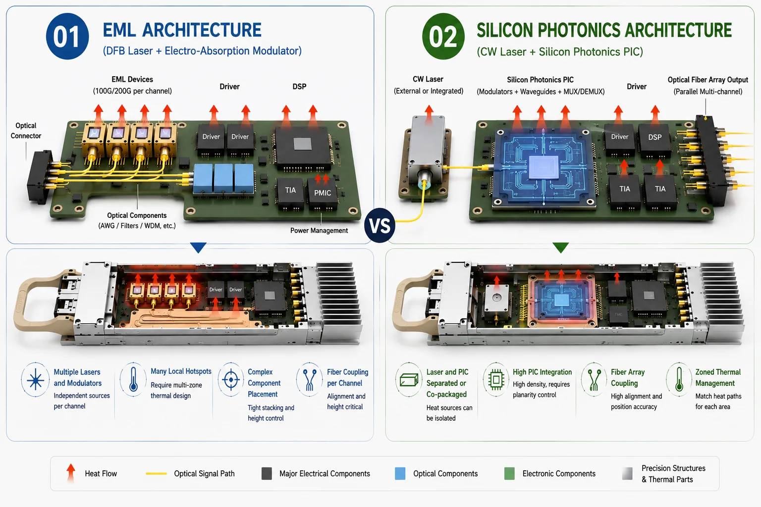
| Light source and modulation | DFB laser and electro-absorption modulator integrated in an InP device | Modulators, waveguides and multiplexing integrated in a silicon PIC; the laser is supplied or integrated separately |
| Optical-engine layout | Multiple EML channels with corresponding drivers | A multi-channel PIC with CW, hybrid or on-die integrated lasers |
| Heat distribution | Several local EML, driver and DSP hotspots | PIC, laser, driver and DSP hotspots may be separated |
| Fiber interface | Discrete coupling followed by multiplexing, or parallel optics | Fiber-array coupling to the PIC is common |
| Structural focus | Multi-device positioning, local heat spreading and channel-height consistency | Optical-engine datums, PIC support, laser position and fiber-strain control |
| Production focus | Device consistency, coupling, thermal steps and multi-channel assembly | PIC packaging, laser integration, fiber arrays, thermal deformation and yield |
Lumentum describes its EMLs as wavelength-locked DFB lasers monolithically integrated with electro-absorption modulators, while its 200G PAM4 EML targets 200G-per-lane connectivity. Coherent’s silicon-photonics-based 1.6T module also uses 200G electrical and optical interfaces. The same 1.6T bandwidth class can therefore be implemented with different optical platforms.
Information boundary: This article is based on public product pages and technical announcements available through August 2026. Optical-engine design, laser integration and module structure vary by supplier. A demonstration should not be treated as the released production architecture of every customer, and the article does not imply that Zhongde supplies any company named here.
1. Why are silicon photonics and EML not simple opposing module types?
A complete optical transceiver has at least four functional layers:
Laser source and modulation
→ optical engine and fiber coupling
→ DSP, drivers, TIAs and PCB
→ housing, cooling, interfaces and insertion structure
An EML sits across the first layer and part of the second. It integrates a DFB laser and an electro-absorption modulator on an InP chip, but the complete module still requires drivers, receivers, a DSP, control electronics, optical coupling and mechanical packaging.
Silicon photonics sits mainly in the optical-engine layer. A silicon PIC can integrate modulators, waveguides, splitters, multiplexers and receiver structures, but a laser source must be provided through one of several routes:
- a separate CW laser connected to the PIC;
- a III-V laser hybrid-integrated with the silicon platform;
- an external laser source feeding one or more optical engines;
- an on-die integrated laser array on a specific silicon-photonics platform.
Intel’s silicon-photonics platform publicly describes an on-die integrated laser array that does not require an external laser. Coherent’s high-efficiency CW InP lasers are designed for silicon-photonics modulators in 800G and 1.6T transceivers. Together, these examples show that silicon photonics does not mean laser-free; it means the laser-to-PIC integration boundary can be different.
2. How does an EML generate and modulate light?
An EML normally contains two monolithically integrated regions:
- a DFB laser generates wavelength-controlled continuous-wave light;
- an electro-absorption modulator changes optical transmission according to the electrical data signal and creates the high-speed PAM4 output.
Because the source and modulator are integrated in one InP device, an EML is compact and well suited to high-speed single-mode links. In 800G and 1.6T modules, several 100G or 200G EML channels can be arranged and then connected to parallel fibers or wavelength-multiplexing optics.
2.1 Module-layout impact
A typical EML transmit path is:
DSP
→ driver
→ EML
→ optical coupling or multiplexing
→ fiber interface
This creates several local functional zones:
- EML mounting surfaces;
- short electrical paths from drivers to EMLs;
- coupling and wavelength-multiplexing optics;
- one or more heat sources per channel;
- fiber and connector locating areas.
The structural challenge is therefore not one housing dimension. It is the combined control of channel height, pitch, heat path and assembly tolerance accumulation.
3. How does a silicon-photonics architecture work?
Silicon photonics uses silicon manufacturing processes to create modulators, waveguides, couplers, splitters, multiplexers and some detector structures in a PIC. Several optical channels can be concentrated in one chip or optical engine, reducing the number of discrete optical parts and increasing integration density.
A typical transmit path is:
Laser or external light source
→ silicon PIC
→ drivers and control electronics
→ fiber array
The first block has no universal implementation. The laser may be:
- integrated in the same optical engine;
- hybrid-integrated close to the PIC;
- located elsewhere in the module;
- placed in an external laser source for CPO;
- integrated on die on a specific silicon-photonics platform.
3.1 Higher integration does not remove mechanical precision
Integrating more optical functions in a PIC raises the importance of:
- the relative position of the PIC and fiber array;
- the optical-engine datum relative to the PCB;
- heat paths among the laser, PIC, drivers and DSP;
- fiber exit bend radius and strain relief;
- optical-engine deformation under lid pressure;
- thermal-expansion mismatch across materials.
As optical functions become more concentrated, a local mechanical deformation can affect more channels at the same time. Silicon photonics shifts precision-manufacturing work from many discrete devices toward the optical engine, fiber array and package datums rather than eliminating it.
4. Core engineering differences
| Item | EML | Silicon photonics |
|---|---|---|
| Main material platform | InP | Silicon PIC, with III-V material often used for the laser |
| Modulation | Electro-absorption modulation | Mach-Zehnder, ring or other silicon modulators |
| Laser relationship | DFB laser monolithically integrated with the modulator | External, hybrid or on-die integrated laser implementations |
| Channel integration | Several EML devices arranged together | Multiple channels integrated in one or a few PICs |
| Fiber coupling | Discrete coupling, multiplexing or parallel output | Fiber-array coupling to the PIC is common |
| Hotspot shape | Multiple local EML and driver hotspots | PIC, laser, driver and DSP hotspots may be separated |
| Structural risk | Channel height, device pitch and local heat spreading | PIC flatness, fiber stress, thermal deformation and package datum |
| Production risk | EML consistency, active coupling and channel assembly | PIC yield, laser integration, fiber-array attach and package yield |
This table does not prove that silicon photonics always uses less power or that EML always reaches farther. Final performance depends on:
- link reach and optical budget;
- 100G, 200G or higher lane rate;
- DSP, LPO or other signal-processing architecture;
- laser efficiency and optical loss;
- package format and temperature;
- production yield and cost;
- module and system cooling.
5. How do the hotspots and heat paths differ?
5.1 Typical EML heat path
An EML module often has several transmit channels. Each channel may create EML and driver hotspots, in addition to DSP, power-management and receive-side heat.
EML / driver
→ local carrier or spreader
→ thermal lid
→ TIM
→ external heatsink
Manufacturing priorities include:
- final height of several thermal-contact steps;
- channel-to-channel temperature consistency;
- contact between local spreaders and the lid;
- whether lid pressure disturbs optical parts;
- final thermal-surface condition after finishing.
5.2 Typical silicon-photonics heat path
A silicon-photonics module may place the PIC, drivers, DSP and laser in separate zones or integrate them more tightly in one optical engine.
CW or integrated laser
+ PIC / drivers
+ DSP / TIA
→ one or more heat paths
→ lid, spreader or dedicated cooling structure
Manufacturing priorities include:
- whether the laser and PIC share a heat path;
- flatness and stiffness of the PIC mounting area;
- whether thermal deformation pulls the fiber array;
- whether lid and TIM compression moves the optical engine;
- whether thermal-expansion mismatch creates long-term drift.
The engineering objective is not to label one architecture cooler. It is to make each hotspot-to-system-heatsink path and its mechanical deformation predictable and repeatable.
6. How are the optical engine, base and lid affected?
6.1 EML module priorities
- locations for multiple EML or TOSA devices;
- short driver-to-EML electrical paths;
- multiplexing optics and fiber interfaces;
- local thermal steps and heat-spreading zones;
- channel assembly height and pitch;
- the tolerance chain from the optical port to the module envelope.
6.2 Silicon-photonics module priorities
- the PIC or optical-engine mounting datum;
- fiber-array fixation and strain relief;
- laser position relative to the PIC;
- the tolerance chain among PCB, optical engine and connector;
- local spreaders and lid contact;
- stiffness and deformation through thermal cycling.
In both architectures, the precision base is more than a support part. It establishes the PCB position, optical-engine position, optical-port position, thermal-contact height and module envelope.
7. Which characteristics are true CTQs?
| CTQ | EML focus | Silicon-photonics focus |
|---|---|---|
| Optical-engine mounting surface | Coplanarity and relative height of multiple devices | PIC flatness and support stiffness |
| Thermal-contact height | Several EML and driver steps | Zoned heights for PIC, laser and DSP |
| PCB and connector location | Electrical path and front interface | Tolerance chain among PIC, DSP and optical port |
| Fiber-interface location | Coupling and multiplexing alignment | Fiber-array position and angle |
| Lid flatness | Uniform TIM and multi-hotspot contact | Pressure and deformation over the PIC zone |
| Finishing boundary | Thermal, ground and optical zones | Thermal, fiber, ground and cleanliness zones |
| Assembled warpage | Load on multi-channel devices | PIC and fiber-array alignment drift |
| Cleanliness | Coupling optics and connectors | PIC, fiber array and optical ports |
A CTQ is not simply the dimension with the smallest tolerance. It is a characteristic whose loss of control breaks an optical, electrical, thermal or mechanical functional loop.
8. Which problems appear during production rather than in prototypes?
8.1 Common EML risks
- manual adjustment can compensate channel-height variation in a few prototypes but not in volume;
- tolerance accumulation among EMLs, drivers and optics shifts coupling positions;
- a local high point on the lid leaves some TIM zones under-compressed;
- device-lot variation changes hotspot balance and temperature uniformity;
- coating thickness changes mounting steps or grounding areas;
- inadequate cleaning or packaging contaminates optical interfaces.
8.2 Common silicon-photonics risks
- a PIC mounting surface passes in the free state but bends after assembly;
- residual stress from fiber-array attach pulls the optical interface;
- laser-to-PIC thermal-expansion mismatch creates thermal-cycle drift;
- lid pressure moves the optical engine;
- blank or thin-wall housing distortion shifts optical-engine datums;
- particles enter the PIC, fiber-array or thermal-contact region.
These risks show why a prototype that powers up and passes a link test is not proof of a stable production process. The acceptance state must be frozen jointly by optical, electrical, thermal, structural and assembly teams.
9. How should the design move from prototype to production?
A practical route is:
Confirm optical architecture and laser location
→ freeze functional datums and CTQs
→ review heat paths and assembly tolerance chains
→ build all-CNC engineering prototypes
→ validate optical, electrical, thermal and insertion functions
→ select blank and production process
→ machine critical functional surfaces
→ finish, clean and mask
→ run pilot production and process-capability review
→ stabilize production and change control
9.1 Prototype phase
All-CNC parts support:
- rapid optical-engine location changes;
- thermal-step and lid-height adjustments;
- fiber-exit and connector-space validation;
- comparison of heat-spreader layouts;
- measurement-datum and assembly-fixture development.
9.2 Production phase
After the design is frozen, evaluate:
- die-cast or forged blanks plus critical CNC finishing;
- aluminum extrusion plus cut-off and local machining;
- stamped, forged or composite copper and aluminum spreaders;
- stamped, cast or molded pull-tab and latch parts;
- dedicated fixtures, automated inspection and mistake-proof assembly.
The production route should be selected by tooling investment, CTQ capability, yield, finishing and design-change frequency, not by unit machining price alone.
10. Where can Zhongde participate?
10.1 Suitable scope
- precision aluminum and copper housings, bases and thermal lids;
- mounting structures around EML or silicon-photonics optical engines;
- metal housings and thermal structures for CW or external laser sources;
- heat spreaders, external heatsinks and local cooling bases;
- CNC finishing of die-cast, extruded, forged or other near-net blanks;
- anodizing, electroless nickel, coating and local masking;
- deburring, cleaning, protective packaging and traceability;
- subassembly, CMM inspection and tolerance-chain validation;
- process transfer from engineering prototypes to batch production.
10.2 Scope that should not be overstated
Zhongde should not claim to provide:
- EML, DFB-laser or silicon-PIC design and wafer fabrication;
- driver, TIA, DSP or high-speed PCB design;
- active fiber alignment and core optical packaging;
- complete optical and electrical transceiver certification;
- IEEE, OIF or MSA certification;
- an existing supply relationship with technology companies mentioned in this article.
A clear boundary helps customers introduce manufacturing support at the right point: structural design freeze, DFM, prototype machining, finishing and production transfer.
11. What inputs should an RFQ include?
| RFQ input | Purpose |
|---|---|
| 2D drawings and 3D models | Confirm dimensions, tolerances, datums and assembly space |
| EML or silicon-photonics architecture | Identify optical-engine and component layout |
| Laser, PIC, driver and DSP locations | Build the hotspot and heat-path map |
| PCB, optical-engine and connector assembly | Build the tolerance chain |
| Power, thermal-contact and TIM requirements | Define lid steps and inspection methods |
| Fiber-array or optical-port location | Define openings, support and cleanliness boundary |
| Key CTQs and acceptance state | Separate machined, finished and assembled acceptance |
| Material, blank and finish | Compare all-CNC, die-cast, extrusion and other routes |
| Prototype and annual volume | Evaluate tooling and automation |
| Cleanliness, packaging and traceability | Protect optical and thermal functional surfaces |
Earlier access to the real assembly state and functional inputs prevents unnecessary tight tolerances on ordinary dimensions while directing control toward the true CTQs.
Frequently asked questions
What is the main difference between silicon-photonics and EML optical transceivers?
An EML integrates a DFB laser and an electro-absorption modulator in one InP transmitter device. Silicon photonics primarily integrates modulators, waveguides, multiplexing and some receiver functions in a silicon photonic integrated circuit. Silicon photonics still needs a laser source, which may be an external CW laser, a hybrid-integrated laser or an on-die integrated laser array on a specific platform. Both architectures are combined with DSPs, drivers, TIAs, PCBs, fiber interfaces and mechanical structures to form a complete transceiver.
Does a silicon-photonics transceiver operate without any laser?
No. A silicon-photonics chip can integrate modulators and optical routing, but the optical signal must still be generated by a laser. Some designs use a separate CW laser or external laser source, some hybrid-integrate a III-V laser with the silicon platform, and platforms such as Intel have publicly described on-die integrated laser arrays. Structural and thermal reviews must therefore identify the actual laser location rather than relying only on the silicon-photonics label.
How do silicon-photonics and EML architectures change the thermal structure?
An EML design often has several EML and driver devices forming distributed local hotspots, so multiple thermal steps, height differences and channel-to-channel temperature consistency must be controlled. A silicon-photonics design may concentrate optical functions in a PIC while locating the CW laser, drivers, DSP and receiver devices in different areas. It therefore places more emphasis on the optical-engine datum, the heat path between the PIC and laser, fiber-array stability and the effect of thermal deformation on optical alignment. The actual requirements depend on the specific module architecture.
What information should be included in an RFQ for silicon-photonics or EML transceiver structures?
Provide 2D drawings and 3D models, the optical architecture, laser and driver locations, PCB and optical-engine assembly relationships, heat-source power and contact areas, TIM requirements, fiber-interface locations, key CTQs, finishing zones, assembly and acceptance states, prototype quantity, expected annual volume, cleanliness and packaging requirements. These inputs allow the supplier to choose between all-CNC, die-cast or other near-net routes and to define the final inspection method.